In solid-state physics, the electronic band structure (or simply band structure) of a solid describes ranges of energy that an electron is "forbidden" or "allowed" to have. It is due to the diffraction of the quantum mechanical electron waves in the periodic crystal lattice. The band structure of a material determines several characteristics, in particular its electronic and optical properties.
Why bands occur in materials
The electrons of a single isolated atom occupy atomic orbitals, which form a discrete set of energy levels. If several atoms are brought together into a molecule, their atomic orbitals split, as in a coupled oscillation. This produces a number of molecular orbitals proportional to the number of atoms. When a large number of atoms (of order × 1020 or more) are brought together to form a solid, the number of orbitals becomes exceedingly large, and the difference in energy between them becomes very small, so the levels may be considered to form continuous bands of energy rather than the discrete energy levels of the atoms in isolation. However, some intervals of energy contain no orbitals, no matter how many atoms are aggregated, forming band gaps.Within an energy band, energy levels are so numerous as to be a near continuum. First, the separation between energy levels in a solid is comparable with the energy that electrons constantly exchange with phonons (atomic vibrations). Second, it is comparable with the energy uncertainty due to the Heisenberg uncertainty principle, for reasonably long intervals of time. As a result, the separation between energy levels is of no consequence.
Basic concepts
Any solid has a large number of bands. In theory, it can be said to have infinitely many bands (just as an atom has infinitely many energy levels). However, all but a few lie at energies so high that any electron that reaches those energies escapes from the solid. These bands are usually disregarded.Bands have different widths, based upon the properties of the atomic orbitals from which they arise. Also, allowed bands may overlap, producing (for practical purposes) a single large band.
Figure 1 shows a simplified picture of the bands in a solid that allows the three major types of materials to be identified: metals, semiconductors and insulators.
Metals contain a band that is partly empty and partly filled regardless of temperature. Therefore they have very high conductivity.
The lowermost, almost fully occupied band in an insulator or semiconductor, is called the valence band by analogy with the valence electrons of individual atoms. The uppermost, almost unoccupied band is called the conduction band because only when electrons are excited to the conduction band can current flow in these materials. The difference between insulators and semiconductors is only that the forbidden band gap between the valence band and conduction band is larger in an insulator, so that fewer electrons are found there and the electrical conductivity is lower. Because one of the main mechanisms for electrons to be excited to the conduction band is due to thermal energy, the conductivity of semiconductors is strongly dependent on the temperature of the material.
This band gap is one of the most useful aspects of the band structure, as it strongly influences the electrical and optical properties of the material. Electrons can transfer from one band to the other by means of carrier generation and recombination processes. The band gap and defect states created in the band gap by doping can be used to create semiconductor devices such as solar cells, diodes, transistors, laser diodes, and others.

Symmetry
A more complete view of the band structure takes into account the periodic nature of a crystal lattice using the symmetry operations that form a space group. The Schrödinger equation is solved for the crystal, which has Bloch waves as solutions:
 ,
,
where k is called the wavevector, and is related to the direction of motion of the electron in the crystal, and n is the band index, which simply numbers the energy bands. The wavevector k takes on values within the Brillouin zone (BZ) corresponding to the crystal lattice, and particular directions/points in the BZ are assigned conventional names like Γ, Δ, Λ, Σ, etc. These directions are shown for the face-centered cubic lattice geometry in Figure 2.
The available energies for the electron also depend upon k, as shown in Figure 3 for silicon in the more complex energy band diagram at the right. In this diagram the topmost energy of the valence band is labeled Ev and the bottom energy in the conduction band is labeled Ec. The top of the valence band is not directly below the bottom of the conduction band (Ev is for an electron traveling in direction Γ, Ec in direction X), so silicon is called an indirect gap material. For an electron to be excited from the valence band to the conduction band, it needs something to give it energy Ec – Ev and a change in direction/momentum. In other semiconductors (for example GaAs) both are at Γ, and these materials are called direct gap materials (no momentum change required). Direct gap materials benefit the operation of semiconductor laser diodes.
Anderson's rule is used to align band diagrams between two different semiconductors in contact.

Figure 2: First Brillouin zone of FCC lattice showing symmetry labels

Figure 3. Bulk band structure for Si,Ge,GaAs and InAs generated with tight binding model. Note that Si and Ge are indirect while GaAs and InAs are direct band gap materials.
Band structures in different types of solids
Although electronic band structures are usually associated with crystalline materials, quasi-crystalline and amorphous solids may also exhibit band structures. However, the periodic nature and symmetrical properties of crystalline materials makes it much easier to examine the band structures of these materials theoretically. In addition, the well-defined symmetry axes of crystalline materials makes it possible to determine the dispersion relationship between the momentum (a 3-dimension vector quantity) and energy of a material. As a result, virtually all of the existing theoretical work on the electronic band structure of solids has focused on crystalline materials.
Density of states

Filling of bands
Although the number of states in all of the bands is effectively infinite, in an uncharged material the number of electrons is equal only to the number of protons in the atoms of the material. Therefore not all of the states are occupied by electrons ("filled") at any time. The likelihood of any particular state being filled at any temperature is given by Fermi-Dirac statistics. The probability is given by the following expression:
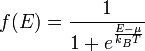
where:
- kB is Boltzmann's constant,
- T is the temperature,
- µ is the chemical potential (in semiconductor physics, this quantity is more often called the "Fermi level" and denoted EF).
The Fermi level naturally is the level at which the electrons and protons are balanced.
At T=0, the distribution is a simple step function:

At nonzero temperatures, the step "smooths out", so that an appreciable number of states below the Fermi level are empty, and some states above the Fermi level are filled.
Band structure of crystals
Brillouin zone
Because electron momentum is the reciprocal of space, the dispersion relation between the energy and momentum of electrons can best be described in reciprocal space. It turns out that for crystalline structures, the dispersion relation of the electrons is periodic, and that the Brillouin zone is the smallest repeating space within this periodic structure. For an infinitely large crystal, if the dispersion relation for an electron is defined throughout the Brillouin zone, then it is defined throughout the entire reciprocal space.
Theory of band structures in crystals
The ansatz is the special case of electron waves in a periodic crystal lattice using Bloch waves as treated generally in the dynamical theory of diffraction. Every crystal is a periodic structure which can be characterized by a Bravais lattice, and for each Bravais lattice we can determine the reciprocal lattice, which encapsulates the periodicity in a set of three reciprocal lattice vectors (b1,b2,b3). Now, any periodic potential V(r) which shares the same periodicity as the direct lattice can be expanded out as a Fourier series whose only non-vanishing components are those associated with the reciprocal lattice vectors. So the expansion can be written as:

where K = m1b1 + m2b2 + m3b3 for any set of integers (m1,m2,m3).
From this theory, an attempt can be made to predict the band structure of a particular material, however most ab initio methods for electronic structure calculations fail to predict the observed band gap.

No hay comentarios:
Publicar un comentario